⚠ 转载请注明出处:作者:ZobinHuang,更新日期:Mar.31 2021

本作品由 ZobinHuang 采用 知识共享署名-非商业性使用-禁止演绎 4.0 国际许可协议 进行许可,在进行使用或分享前请查看权限要求。若发现侵权行为,会采取法律手段维护作者正当合法权益,谢谢配合。
This Project Had Won National Second Prize of NUEDC (2019)
1. Basic Requirement of The Project
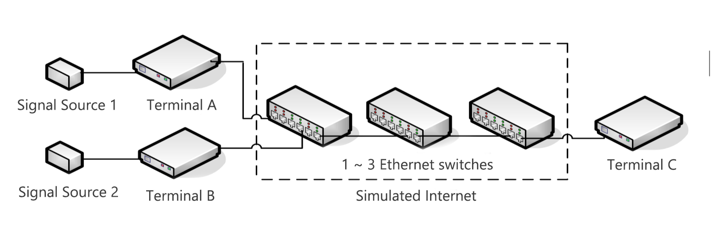
As shown in the figure :
Design and make three terminal nodes (both software and hardware) that can access the Ethernet.Terminal A and B are used for signal sampling (The collected signal is a periodic AC signal with a peak-to-peak range of 1V ~ 5V, sampling rate shouldn’t less than 10MS / s, and the number of sampling bits shouldn’t less than 8. Terminal C which receive the signal data transported from terminal A and B is used for signal regeneration (both two signals). By measuring and compensating the delay of the transmission network, the phase of regeneration signal should synchronize with the original signal’s. Maximum synchronization error time (including jitter) of two regeneration signal periods should not greater than 10 microseconds. By changing the number of cascaded switches or the length of the network cable to change the network delay, terminal C should automatically measure and compensate the delay time to achieve fast synchronization between the phase of the regenerative signal and the original signal. Starting from the connection of the network cable, the maximum synchronization error time (including jitter) of the two signal periods shouldn’t more than 10 microseconds, and the time is not more than 5 seconds.
2. Solution
(1) Basic principles of precise network synchronization
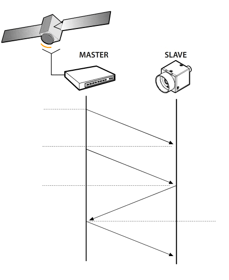
Due to the NTP (Network Time Protocol) cannot achieve the subtle level of precision required by the project, we have implemented PTP (Precision Time Protocol) as the basis of the project. The basic principle of PTP is as follows:
There is one master clock and several slave clocks in the network. After running PTP, the time synchronization among the slave clock and the master clock will be achieved. The implementation process is as follows:
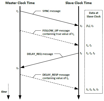
1)The master clock periodically sends sync messages, and records the precise sending time of the Sync Message leaving the master clock as t1.
2) The master clock encapsulates the precise transmission time t1 into a Follow_up Message and sends it to the slave clock.
3) The slave clock records the time when the sync message arrived at the slave clock as t2.
4) Send a Delay_req Message from slave clock and record the exact sending time t3.
5) The master clock records the precise arrival time of the delay_req message to the master clock as t4.
6) The master clock sends a Delay_resp Message with accurate time stamp information t4 to the slave clock.
In this way, the slave clock obtained four precise times such as t1, t2, t3 and t4.
So the Time Offset between master and slave clocks can be calculated as:
The internet delay between master and slave clock can be calculated as:
Therefore, in our system, the master clock is terminal C that is responsible for reconstructing the signal, and the slave clock are terminal A and terminal B that are responsible for signal sampling. The time stamp recorded by the terminal should be a hardware time stamp to ensure synchronization accuracy. Running such a set of protocols in these three terminals can realize the time synchronization among terminals, and eventually realize the phase synchronization of both two signals’ regeneration.
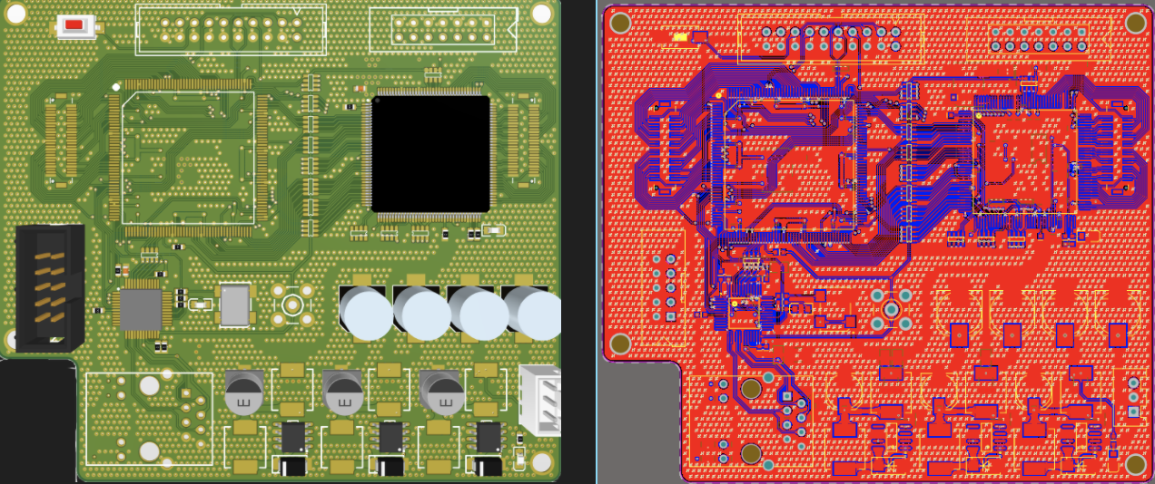
(2) Design of terminal structure
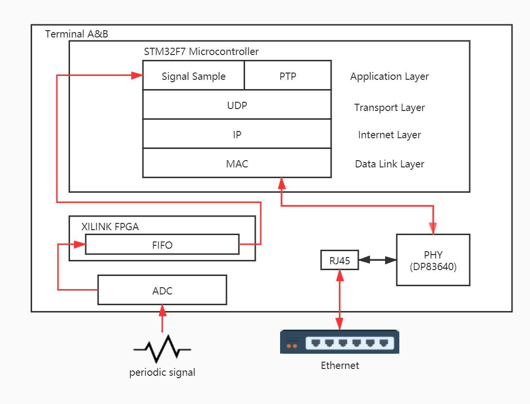
Design of terminal A & B:
Design of terminal C:

(a) Hardware Part
As shown in the figure,
We used STM32F7 as the terminal controller. For terminal A and terminal B, the project requires a sampling rate of no less than 10 Mb/s and a sampling bit number of no less than 8 bits. We worried that the STM32F7's I/O read speed and storage capacity cannot accept such a large amount of data and high transmission rate requirements, so my teammate who in charge of hardware part designed a FIFO structure in the FPGA which is responsible for controlling the ADC sampling and storing the sampling point data. FPGA would communicate with STM32F7 through the FSMC interface to meet the sampling rate and sampling bit requirements. For terminal C, we also designed two FIFO structures in the FPGA to store the signal sample data from terminal A and B.
According to IEEE1588, we used DP83640 as the PHY chip. Since the chip has the function of adding or extracting hardware timestamp to the message, the hardware-level timestamp provides the system with sufficient accuracy to implement the synchronization. Due to the MII interface uses four parallel data lines to transmit physical layer data between MAC and PHY, we used the MII interface to connect the STM32F7 and the PHY chip to reduce the connection transmission rate and the difficulty of PCB design.
For ADC and DAC chips, we have selected devices that meet the project sampling rate and number of bits.
(ab Software Part
We ported the LwIP stack to STM32F7 to access the TCP / IP network, and the protocol stack completed the basic functions of the transport layer, network layer, and data link layer.
Based on the protocol stack, we designed two modules on the application layer: one is the module responsible for communicating with the FPGA and receiving sampling data. The operations of the FSMC interface are used to obtain data from several sampling points, and then encapsulate them in the same UDP packet and send it to terminal C. The other is a module responsible for implementing the PTP synchronization function. Based on the above-mentioned PTP principle, we designed the clock synchronization process of the terminal as follows:
Take terminal A as an example:
(1) After the terminal is turned on, the runtime of the terminal starts counting from 0 (The controller of three terminals is isomorphic, so the frequency of the external crystals are the same. That means the clock rate of three terminals are the same)
(2) Terminal C and terminal A perform a round of PTP message interaction (described above). Terminal A obtains four accurate hardware timestamps and corrects its system runtime and measures the network delay according to the formula given above.
(3) Terminal A informs terminal C of the network delay.
We believed that the system should periodically maintain such a synchronization process in order to ensure the clock synchronization among terminals for a long time and have the ability to cope with various network topology changes that may occur.
After the terminal clock synchronization is completed, the signal sampling data is transmitted. Each group of sampling points corresponds to a sampling time of 0.0001s (1000 sampling points at a sampling rate of 10M). Terminal A / B would record the start of each group. The sampling time at the starting sampling point would be encapsulated in a data packet to inform the terminal C. The terminal C uses a DAC module to recover the sampling signals from A and B at a specific time according to the starting time value, thereby achieving phase synchronization of the sampling signals.
In addition, we also completed the coding of related hardware peripheral drivers, and finally completed the design of entire system.
3. Survey
After this project, I
(a) Learned how to transplant the LwIP protocol stack on the embedded system and track the encapsulation and decapsulation process of message information in the protocol stack during the debugging process. Get familiar with the basic architecture of the protocol stack
(b) Mastered the synchronization algorithm of PTP. After writing the DP83640 PHY chip driver, the hardware time stamp can be used and in conjunction with the protocol stack to complete the PTP process and realize the timing synchronization of the network terminals.
(c) Got familiar with the use of the surrounding hardware resources of the embedded system. Besides the porting of embedded network protocol stack, the peripheral drivers such as ADC, DAC, FSMC interface, and PHY have been written to realize the integration of system hardware resources.
(d) Cooperation with teammates is very important. Software designers and hardware designers must constantly communicate to design an efficient system.
4. Award
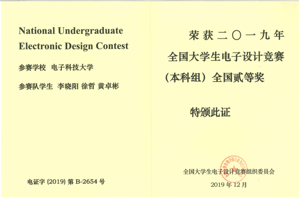
The system won the national second prize of NUEDC for its stability and high efficiency. (Top 5% in the country)
5. Appreciation
1. Specially thanks to Professor Zhongxiao Yang & Professor Zhuming Chen. We couldn't complete this system without their guidance.
2. Specially thanks to my teammate Xu. Without his efforts, the hardware platform would not be successfully developed. My efforts in software would be useless.